Forth Computing on FPGA
| Sponsors |
|
| Team Name | FORTH Generation |
| Duration | 2019 - 2020 |
| Faculty Adviser |
|
| Client |
|
| Team Members |
|
The goal of this project is to develop an Arduino-like board/platform based upon an FPGA-based soft-CPU with an instruction set tooled specifically FORTH. The hardware i
The product, the F18 processor, is a soft-CPU designed in Verilog based off of the J1 CPU designed by James Bowman. Unlike the J1, the CPU has an 18-bit instruction set so that relative jump and call instructions could easily be added to the instruction set. Also implemented was a UART interface and a specialized VGA interface for running a simple game of Pong.
Problem Definition[edit | edit source]
Background[edit | edit source]
FORTH is a very small interpreted programming language that was originally developed for controlling scientific instrumentation. The FORTH language is quite low level and looks very much like assembly code (but for a stack machine), but FORTH also offers high-levels of abstraction and modularity with its metaprogramming capabilities.
A custom designed soft-CPU that executes FORTH instructions on an FPGA is a very versatile, low power, and small form factor way to accomplish many computing tasks.
Our design, called the F18, is ideal for applications with many arithmetic calculations, high data throughput, or as a controller for designs with other subsystems.
Specifications[edit | edit source]
The specifications of this project were pretty general: to create a custom soft-CPU that runs FORTH instructions. Another specification added later in the design process was to be able to run a game of Pong on 1280x1024 VGA screen.
Design Considerations[edit | edit source]
While considering the modifications to make to the J1, we considered additions such as relative branches and calls, interrupts, a loop stack, and a conditional branch instruction for != 0. The changes that we ended up making were adding relative branches and calls. This required that we increase the size of our instructions to 18 bits.
Another consideration we made is what FPGA board we would target. We ended up targeting the Alorium Hinj board over the Alorium XLR8 board due its feature set and easy expansion.
Final Design[edit | edit source]
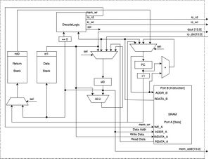
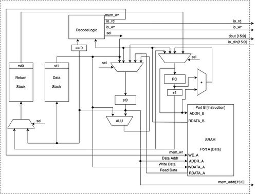
The final design is design specifically for running FORTH. Because of this, many of the common FORTH words can be executed in only one instruction cycle. It has two RAM-based LIFO stack with a depth of 512 and a width of 16 bits: the data stack where data manipulation and calculation is done and the return stack where return addresses for function calls are stored. In the J1, the stacks were implemented using register arrays, but we opted for RAM stacks in our design in order to reduce the number of flip flops used while also increasing the depth of the stacks.
The design has, unlike the J1 design, an 18-bit instruction width. This was done in order to add the capability of relative jumps and calls. This also leaves room for additional instructions to be added in the future if desired. The design uses a true dual port 8Kx18 SRAM for data and program storage. Port A of the SRAM is used for reading and writing data while port B is a read-only port which is used for fetching processor instructions. Both read buses for each port are individual inputs of the processor. The design clocks at 16 MHz.
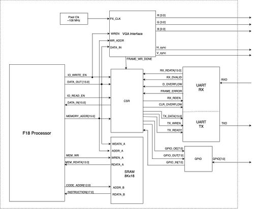
There are three primary I/O interfaces: VGA, UART, and GPIO. The VGA interface allows for sprite location and image data to be written to a VGA monitor from the processor. Although the module was design for the display of sprites for a simple Pong game, this module could be easily modified in the future for other purposes. The UART allows for general data communication. The 8 GPIO pins can be configured to control external devices such as stepper motors, LEDs, etc. or receive additional data.
The F18 processor has one general 16-bit data output bus and one general 16-bit address bus which both connect to the VGA interface, the control/status register (CSR) module, and the system memory. The CSR module’s purpose is to decode the address signal and IO read/write signals to determine what I/O data the processor is attempting to read or write. The VGA interface is connected directly to the processor’s data out bus and IO write bus because it contains internal hardware to determine if it is being written to. The VGA interface does pass one signal back to the CSR which indicates that the information for all images on a screen has been committed and can then be passed new values from the F18.
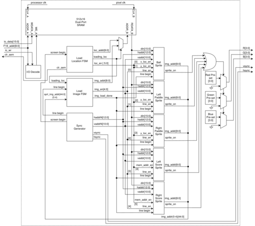
The design is equipped with a VGA interface which is currently geared toward displaying the game Pong. The VGA hardware displays 5 different sprites currently, a ball, two paddles and two score values. The interface is set to run 1280x1024 screen at a 60 Hz refresh rate.
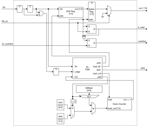
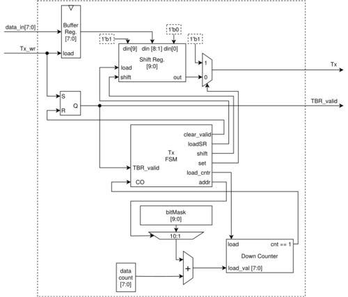
The system is equipped with a UART for receiving and transmitting data to and from other devices. The UART is hardcoded for 8 data bits, 1 start bit, 1 stop bit, and no parity bits. A more robust design could have been implemented; however, it was not necessary and thus a simple UART both conserves hardware resources and meets the needs of the system. The baud rate currently is also hardcoded into the Verilog for 115.2 kBps.
A prototype of the Pong game can be seen here
Validation[edit | edit source]
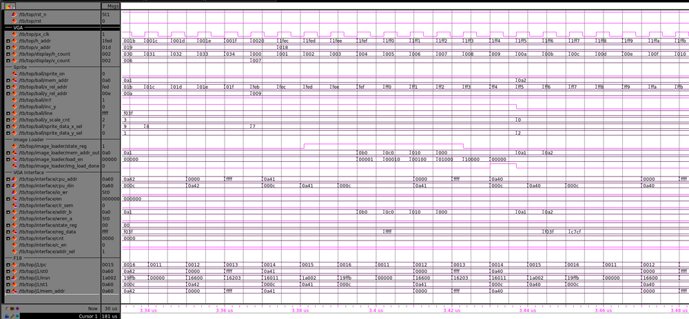
Logic analyzer waveforms were used regularly to observe the functionality of different design elements. This shows sprite data being loaded from RAM to an internal register to be later drawn to the screen.
Team Members[edit | edit source]
|
Name: Jess Totorica
|
Name: Kyle Hartman
|
Name: Thys Ballard | |||
|
Name: Kyle Hild |
Name: Ronald Crump |
Additional Documentation[edit | edit source]
See Github page
